Structure
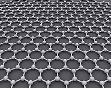
Graphene is a crystalline allotrope of carbon with 2-dimensional properties. Its carbon atoms are densely packed in a regular atomic-scale chicken wire (hexagonal) pattern.
Each atom has four bonds, one σ bond with each of its three neighbors and one π-bond that is oriented out of plane. The atoms are about 1.42 Å apart.
Graphene's hexagonal lattice can be regarded as two interleaving triangular lattices. This perspective was successfully used to calculate the band structure for a single graphite layer using a tight-binding approximation.
Graphene's stability is due to its tightly packed carbon atoms and a sp2 orbital hybridization – a combination of orbitals s, px and py that constitute the σ-bond. The final pz electron makes up the π-bond. The π-bonds hybridize together to form the π-band and π∗-bands. These bands are responsible for most of graphene's notable electronic properties, via the half-filled band that permits free-moving electrons.
Graphene sheets in solid form usually show evidence in diffraction for graphite's (002) layering. This is true of some single-walled nanostructures. However, unlayered graphene with only (hk0) rings has been found in the core of presolar graphite onions. TEM studies show faceting at defects in flat graphene sheets and suggest a role for two-dimensional crystallization from a melt.
Graphene can self-repair holes in its sheets, when exposed to molecules containing carbon, such as hydrocarbons. Bombarded with pure carbon atoms, the atoms perfectly align into hexagons, completely filling the holes.
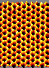
The atomic structure of isolated, single-layer graphene was studied by transmission electron microscopy (TEM) on sheets of graphene suspended between bars of a metallic grid. Electron diffraction patterns showed the expected honeycomb lattice. Suspended graphene also showed "rippling" of the flat sheet, with amplitude of about one nanometer. These ripples may be intrinsic to the material as a result of the instability of two-dimensional crystals, or may originate from the ubiquitous dirt seen in all TEM images of graphene. Atomic resolution real-space images of isolated, single-layer graphene on SiO2 substrates are available[67] via scanning tunneling microscopy. Photoresist residue, which must be removed to obtain atomic-resolution images, may be the "adsorbates" observed in TEM images, and may explain the observed rippling. Rippling on SiO2 is caused by conformation of graphene to the underlying SiO2, and is not intrinsic.
Applications
As of 2015, there is one product available for commercial use, a graphene-infused printer powder. Many other uses for graphene have been proposed or are under development, in areas including electronics, biological engineering, filtration, lightweight/strong composite materials, photovoltaics and energy storage. Graphene is often produced as a powder and as a dispersion in a polymer matrix. This dispersion is supposedly suitable for advanced composites, paints and coatings, lubricants, oils and functional fluids, capacitors and batteries, thermal management applications, display materials and packaging, solar cells, inks and 3D-printers’ materials, and barriers and films.

Scanning probe microscopy image of graphene

Graphene is an atomic-scale honeycomb lattice made of carbon atoms.
Products
GRAPHENE DERIVATIVES
2D SOLUTIONS
2D POWDERS
2D TOPOLOGICAL INSULATORS
2D ALLOYS
DOPED 2D SEMICONDUCTORS
2D SEMICONDUCTORS
2D METALS-SUPERCONDUCTORS
2D INSULATORS
The Summit-Tech Company is an ISO:9001-2015 certified company. Copyright ©1996-2016 Summit-Tech Company® All rights reserved.
