Materials news
New technique can measure electronic properties of 2D materials
Electronic devices are set to become flexible, highly efficient and much smaller, following a breakthrough in measuring two-dimensional 'wonder' materials by researchers at the University of Warwick in the UK. Neil Wilson in the Department of Physics has developed a new technique for measuring the electronic structures of stacks of two-dimensional (2D) materials – flat, atomically thin, highly conductive and extremely strong materials – for the first time. The new technique is described in a paper in Science Advances.
Multiple stacked layers of 2D materials – known as heterostructures – can create highly efficient optoelectronic devices with ultrafast electrical charge. Such stacked layers can be used in nano-circuits and are stronger than the materials used in traditional circuits. Various heterostructures have been created using different 2D materials, and stacking different combinations of 2D materials creates new materials with new properties.
Wilson's technique measures the electronic properties of each layer in a stack, allowing researchers to establish the optimal structure for the fastest, most efficient transfer of electrical energy. The technique uses the photoelectric effect to directly measure the momentum of electrons within each layer and shows how this momentum changes when the layers are combined.
The ability to understand and quantify how 2D material heterostructures work – and to create optimal semiconductor structures – paves the way for the development of highly efficient nano-circuitry, and smaller, flexible, more wearable devices. Solar power could also be revolutionized by heterostructures, as the atomically-thin layers allow for strong absorption and efficient power conversion with a minimal amount of photovoltaic material.
"It is extremely exciting to be able to see, for the first time, how interactions between atomically-thin layers change their electronic structure," says Wilson. "This work also demonstrates the importance of an international approach to research; we would not have been able to achieve this outcome without our colleagues in the USA and Italy."
Wilson formulated the technique in collaboration with colleagues in the theory groups at the University of Warwick and the University of Cambridge in the UK, at the University of Washington in Seattle, and the Elettra Light Source, near Trieste in Italy. In addition, understanding how interactions between the atomic layers alter their electronic structure required the help of computational models developed by Nick Hine, also from Warwick's Department of Physics.
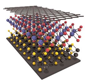
This is an artist’s illustration of a heterostructure made up of two-dimensional 'wonder' materials. Image: Gabriel Constantinescu.
Ferroelectric materials can generate power from ‘hot’ electrons
12 August 2016
New perovskite solar cell design could outperform existing commercial technologies
High-efficiency tandem cells created
A new design for solar cells that uses inexpensive, commonly available materials could rival and even outperform conventional cells made of silicon.
Writing in the Oct. 21 edition of Science, researchers from Stanford and Oxford describe using tin and other abundant elements to create novel forms of perovskite -- a photovoltaic crystalline material that's thinner, more flexible and easier to manufacture than silicon crystals.
"Perovskite semiconductors have shown great promise for making high-efficiency solar cells at low cost," said study co-author Michael McGehee, a professor of materials science and engineering at Stanford. "We have designed a robust, all-perovskite device that converts sunlight into electricity with an efficiency of 20.3 percent, a rate comparable to silicon solar cells on the market today."
The new device consists of two perovskite solar cells stacked in tandem. Each cell is printed on glass, but the same technology could be used to print the cells on plastic, McGehee added.
"The all-perovskite tandem cells we have demonstrated clearly outline a roadmap for thin-film solar cells to deliver over 30 percent efficiency," said co-author Henry Snaith, a professor of physics at Oxford. "This is just the beginning."
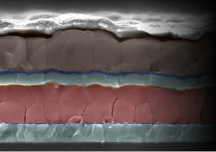
Cross-section of a new tandem solar cell designed by Stanford and Oxford scientists. The brown upper layer of perovskite captures low-energy lightwaves, and the red perovskite layer captures high-energy waves.
Credit: Scanning electron microscopy image by Rebecca Belisle and Giles Eperon
A recent discovery by a team of researchers has revealed that a class of materials known as ferroelectrics could be better at converting sunlight into energy than the materials currently being used in solar arrays. The team’s research shows how this class of materials can extract power from a small portion of the sunlight spectrum with an efficiency that is above its theoretical maximum – a value known as the Shockley-Queisser limit. This finding, which could lead to more power-efficient solar cells, was inspired by a near-half-century old discovery by Russian physicist Vladimir Fridkin, a visiting professor of physics at Drexel University and one of the innovators behind the photocopier.
The team, which includes scientists from Drexel University, the Shubnikov Institute of Crystallography of the Russian Academy of Sciences, the University of Pennsylvania and the US Naval Research Laboratory recently published its findings in Nature Photonics. Their paper explains how they were able to use the ferroelectric barium titanate to convert sunlight into electrical power much more efficiently than the Shockley-Queisser limit would dictate for a material that absorbs almost no light in the visible spectrum – only ultraviolet wavelengths.

This is an artist's conception of light-generated non-thermalized electrons and their collection in a ferroelectric crystal. An intense screening field results in impact ionization, producing an unexpectedly high conversion efficiency. Image: Ella Marushchenko.
The foundation for the new findings was observed by Fridkin, who is one of the principal co-authors of the paper, some 47 years ago. This is when he discovered a physical mechanism for converting light into electrical power – one that differs from the method currently employed in solar cells. The mechanism relies on collecting ‘hot’ electrons, which contain excess energy that in conventional solar cells is lost as heat rather than converted into electricity. And though it has received relatively little attention until recently, this so-called ‘bulk photovoltaic effect’ might now be the key to revolutionizing our use of solar energy.
Up to now, solar energy conversion has been limited by solar cell design and by the electrochemical characteristics of the materials used to make solar cells.
"In a conventional solar cell – made with a semiconductor – absorption of sunlight occurs at an interface between two regions, one containing an excess of negative-charge carriers, called electrons, and the other containing an excess of positive-charge carriers, called holes," explained Alessia Polemi, a research professor in Drexel's College of Engineering and one of the co-authors of the paper.
In order to generate electron-hole pairs at the interface, which is necessary for producing an electric current, the photons in sunlight must excite the electrons so that they vacate the semiconductor’s valence band and move into the conduction band. The difference in energy levels between these two bands is referred to as the ‘band gap’.
Photons in sunlight with energies that are greater than the band gap produce excited electrons with corresponding excess energy, which is lost as heat rather than converted into electric current. This process reduces the amount of power that can be extracted from a solar cell.
"The light-induced carriers generate a voltage, and their flow constitutes a current. Practical solar cells produce power, which is the product of current and voltage," Polemi said. "This voltage, and therefore the power that can be obtained, is also limited by the band gap."
But, as Fridkin discovered in 1969 – and the team validates with this research – this limitation is not universal, which means solar cells can be improved.
When Fridkin and his colleagues at the Institute of Crystallography in Moscow observed an unusually high photovoltage while studying the ferroelectric antimony sulfide iodide – a material that does not have any junction separating the carriers – he posited that crystal symmetry could be the origin for its remarkable photovoltaic properties. He later explained how the ‘bulk photovoltaic effect’, which is very weak, transports photo-generated hot electrons in a particular direction without any collisions that could cool the electrons.
This is significant because the limit on solar power conversion specified in the Shockley-Queisser theory is based on the assumption that all of the excess energy is lost – wasted as heat. But the team's discovery shows that not all of the excess energy of hot electrons is lost, and that the energy can, in fact, be extracted as power before it is converted into heat.
"The main result – exceeding [the energy gap-specific] Shockley-Queisser [power efficiency limit] using a small fraction of the solar spectrum – is caused by two mechanisms," Fridkin said. "The first is the bulk photovoltaic effect involving hot carriers and second is the strong screening field, which leads to impact ionization and multiplication of these carriers, increasing the quantum yield."
Impact ionization, which leads to carrier multiplication, can be likened to an array of dominoes in which each domino represents a bound electron. When a photon interacts with an electron, it excites the electron, which, when subject to a strong field, accelerates and 'ionizes' or liberates other bound electrons in its path, each of which also accelerates and triggers the release of yet more electrons. Like setting off multiple domino cascades with a single tipped tile, this process can generate a much greater electric current.
The second mechanism, the screening field, is an electric field that is present in all ferroelectric materials. The nanoscale electrode used to collect the current in a solar cell enhances this screening field, which has the beneficial effect of promoting impact ionization and carrier multiplication. Following the domino analogy, the field drives the cascade effect, ensuring that it continues from one domino to the next.
"This result is very promising for high efficiency solar cells based on application of ferroelectrics having an energy gap in the higher intensity region of the solar spectrum," Fridkin said.
"Who would have expected that an electrical insulator could be used to improve solar energy conversion?" said Jonathan Spanier, a professor of materials science, physics and electrical engineering at Drexel and one of the principal authors of the study. "Barium titanate absorbs less than a tenth of the spectrum of the sun. But our device converts incident power 50% more efficiently than the theoretical limit for a conventional solar cell constructed using this material or a material of the same energy gap."
This breakthrough also builds on research conducted several years ago by Andrew Rappe, professor of chemistry and of materials science & engineering at the University of Pennsylvania, one of the principal authors, and Steve Young, also a co-author of the new report. Rappe and Young showed how bulk photovoltaic currents could be calculated, which led Spanier and his collaborators to investigate whether a higher power conversion efficiency could be attained in ferroelectrics.
ƒsƒƒ
"There are many exciting reports utilizing nanoscale materials or phenomena for improving solar energy conversion," Spanier said. "Professor Fridkin appreciated decades ago that the bulk photovoltaic effect enables free electrons that are generated by light and have excess energy to travel in a particular direction before they cool or 'thermalize' – and lose their excess energy to vibrations of the crystal lattice."
Rappe was also responsible for connecting Spanier to Fridkin in 2015, a collaboration that set in motion the research now detailed in the Nature Photonics paper – a validation of Fridkin's decades-old vision.
This story is adapted from material from Drexel University, with editorial changes made by Materials Today. The views expressed in this article do not necessarily represent those of Elsevier. Link to original source.
The hot attraction of gold
Date: July 27, 2016
Source: Tohoku University
Summary: Gold had long been considered a non-magnetic metal. But researchers recently discovered that gold can in fact be magnetized by applying heat.
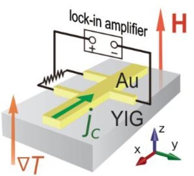
This image shows hall voltage measurement in the bilayer system under the temperature gradient and external magnetic field perpendicular to the bilayer.
Credit: Eiji Saitoh
Gold had long been considered a non-magnetic metal. But researchers at Tohoku University recently discovered that gold can in fact be magnetized by applying heat.
They discovered that an electron spin -- the origin of magnetism -- plays an important role in a material's functionality at a non-constant temperature, where the magnetization and the heat flow interact. A subsequent experiment confirmed, for the first time, that magnetization in gold can be induced by the heat flow driven by a temperature change.
The set up of the experiment was quite simple, involving a bilayer comprising Yttrium iron garnet (YIG), which is an insulator magnet, and a thin film of gold. (Fig below).
In the experiment, the temperature of the YIG side and that of the gold side were kept different to drive a heat flow perpendicular to the bilayer. In addition, a magnetic field was applied in parallel to the heat flow. Under this condition, the Hall voltage*1 was measured in the gold film by in-plane electric current. The Hall voltage showed a clear proportional dependence on the applied temperature gradient.
The team interpreted this Hall voltage as evidence of the evolution of magnetization in the thin gold film due to the heat flow. The Hall voltage was named as a non-equilibrium anomalous Hall effect (nAHE).
"We are excited about the potential of this measurement as a standard method of detecting non-equilibrium magnetization because there's no need for complicated processing and technologies as compared to other highly sensitive magnetometry," says researcher Dazhi Hou. "On top of that, we can detect extremely small magnitudes of magnetization in this measurement. Such small magnetizations is the key to revealing as-yet-unknown useful properties of matters."
"These findings are expected to contribute to the development of innovative spintronics in the use of thermoelectric applications, like energy harvesting, adds Professor Eiji Saitoh, who led the research.
Details of this study were published online on July 26, 2016 in Nature Communications.
This research was achieved as part of JST-ERATO "Spin Quantum Rectification Project" led by Professor Eiji Saitoh.
*1 When passing an electrical current on through a conductor and applying a magnetic field perpendicularly to the direction of the current, an electric voltage will be generated in a direction perpendicular to the current and magnetic field.
Story Source:
The above post is reprinted from materials provided by Tohoku University. Note: Materials may be edited for content and length.
This self-healing material could solve many wearable woes
The physical limitations of existing materials are one of main problems when it comes to flexible electronics, be it wearables, medical or sports tech. If a flexible material breaks, it either stays broken, or if it has some self-healing properties it may continue to work, but not so well. However, a team from Penn State have creating a self-healing, flexible material that could be used inside electronics even after multiple breaks.
The main challenge facing researchers led by Professor Qing Wang, was ensuring that self-healing electronics could restore "a suite of functions". The example used explains how a component may still retain electrical resistance, but lose the ability to conduct heat, risking overheating in a hypothetical wearable, which is never good. The nano-composite material they came up with was mechanically strong, resistant against electronic surges, thermal conductivity and whilst packing insulating properties. Despite being cut it in half, reconnecting the two parts together and healing at a higher temperature almost completely heals where the cut was made. The thin strip of material could also hold up to 200 grams of weight after recovering.
Unlike other healable materials, the boron-nitrate nanosheets the Penn State team used are unaffected by moisture, meaning it could also be used in high humidity environments like the shower. "This is the first time that a self-healable material has been created that can restore multiple properties over multiple breaks, and we see this being useful across many applications," said Qing Wang. "We need conducting elements in circuits but we also need insulation and protection for microelectronics."
IBM Scientists Achieve Storage Memory Breakthrough
Technology can speed up machine learning and access to the Internet of Things, mobile phone apps and cloud storage
Zurich, Switzerland - 17 May 2016: For the first time, scientists at IBM (NYSE: IBM) Research have demonstrated reliably storing 3 bits of data per cell using a relatively new memory technology known as phase-change memory (PCM).


<
>
The current memory landscape spans from venerable DRAM to hard disk drives to ubiquitous flash. But in the last several years PCM has attracted the industry’s attention as a potential universal memory technology based on its combination of read/write speed, endurance, non-volatility and density. For example, PCM doesn’t lose data when powered off, unlike DRAM, and the technology can endure at least 10 million write cycles, compared to an average flash USB stick, which tops out at 3,000 write cycles.
This research breakthrough provides fast and easy storage to capture the exponential growth of data from mobile devices and the Internet of Things.
Applications
IBM scientists envision standalone PCM as well as hybrid applications, which combine PCM and flash storage together, with PCM as an extremely fast cache. For example, a mobile phone’s operating system could be stored in PCM, enabling the phone to launch in a few seconds. In the enterprise space, entire databases could be stored in PCM for blazing fast query processing for time-critical online applications, such as financial transactions.
Machine learning algorithms using large datasets will also see a speed boost by reducing the latency overhead when reading the data between iterations.
How PCM Works
PCM materials exhibit two stable states, the amorphous (without a clearly defined structure) and crystalline (with structure) phases, of low and high electrical conductivity, respectively.
To store a ‘0’ or a ‘1’, known as bits, on a PCM cell, a high or medium electrical current is applied to the material. A ‘0’ can be programmed to be written in the amorphous phase or a ‘1’ in the crystalline phase, or vice versa. Then to read the bit back, a low voltage is applied. This is how re-writable Blue-ray Discs* store videos.
Previously scientists at IBM and other institutes have successfully demonstrated the ability to store 1 bit per cell in PCM, but today at the IEEE International Memory Workshop in Paris, IBM scientists are presenting, for the first time, successfully storing 3 bits per cell in a 64k-cell array at elevated temperatures and after 1 million endurance cycles.
“Phase change memory is the first instantiation of a universal memory with properties of both DRAM and flash, thus answering one of the grand challenges of our industry,” said Dr. Haris Pozidis, an author of the paper and the manager of non-volatile memory research at IBM Research - Zurich. “Reaching 3 bits per cell is a significant milestone because at this density the cost of PCM will be significantly less than DRAM and closer to flash.”
To achieve multi-bit storage IBM scientists have developed two innovative enabling technologies: a set of drift-immune cell-state metrics and drift-tolerant coding and detection schemes.
More specifically, the new cell-state metrics measure a physical property of the PCM cell that remains stable over time, and are thus insensitive to drift, which affects the stability of the cell’s electrical conductivity with time. To provide additional robustness of the stored data in a cell over ambient temperature fluctuations a novel coding and detection scheme is employed. This scheme adaptively modifies the level thresholds that are used to detect the cell’s stored data so that they follow variations due to temperature change. As a result, the cell state can be read reliably over long time periods after the memory is programmed, thus offering non-volatility.
“Combined these advancements address the key challenges of multi-bit PCM, including drift, variability, temperature sensitivity and endurance cycling,” said Dr. Evangelos Eleftheriou, IBM Fellow.
The experimental multi-bit PCM chip used by IBM scientists is connected to a standard integrated circuit board. The chip consists of a 2 × 2 Mcell array with a 4- bank interleaved architecture. The memory array size is 2 × 1000 μm × 800 μm. The PCM cells are based on doped-chalcogenide alloy and were integrated into the prototype chip serving as a characterization vehicle in 90 nm CMOS baseline technology.
OpenPOWER
At the 2016 OpenPOWER Summit in San Jose, CA, last month, IBM scientists demonstrated, for the first time, phase-change memory attached to POWER8-based servers (made by IBM and TYAN® Computer Corp.) via the CAPI (Coherent Accelerator Processor Interface) protocol. This technology leverages the low latency and small access granularity of PCM, the efficiency of the OpenPOWER architecture and the CAPI protocol. In the demonstration the scientists measured very low and consistent latency for 128-byte read/writes between the PCM chips and the POWER8 processor.
For more information on today’s announcement watch this video: https://youtu.be/q3dIw3uAyE8. Continue the conversation at @IBMResearch #3bitPCM.
M. Stanisavljevic, H. Pozidis, A. Athmanathan, N. Papandreou, T. Mittelholzer, and E. Eleftheriou,"Demonstration of Reliable Triple-Level-Cell (TLC) Phase-Change Memory,'' in Proc. International Memory Workshop, Paris, France, May 16-18, 2016
“Multilevel-Cell Phase Change Memory: A Viable Technology” by Aravinthan Athmanathan, Milos Stanisavljevic, Nikolaos Papandreou, Haralampos Pozidis and Evangelos Eleftheriou, is available at DOI: 10.1109/JETCAS.2016.2528598
About IBM Research
For more than seven decades, IBM Research has defined the future of information technology with more than 3,000 researchers in 12 labs located across six continents. Scientists from IBM Research have produced six Nobel Laureates, 10 U.S. National Medals of Technology, five U.S. National Medals of Science, six Turing Awards, 19 inductees in the U.S. National Academy of Sciences and 20 inductees into the U.S. National Inventors Hall of Fame. For more information about IBM Research, visit www.ibm.com/research.
Pioneering research boosts graphene revolution
Source: University of Exeter
Summary:
Pioneering new research could pave the way for miniaturized optical circuits and increased internet speeds, by helping accelerate the 'graphene revolution'.
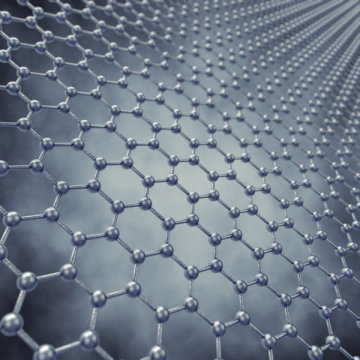
Graphene illustration (stock image). New research could pave the way for miniaturized optical circuits and increased internet speeds.
Credit: © nobeastsofierce / Fotolia
Pioneering new research by the University of Exeter could pave the way for miniaturized optical circuits and increased internet speeds, by helping accelerate the 'graphene revolution'.
Physicists from the University of Exeter in collaboration with the ICFO Institute in Barcelona have used a ground-breaking new technique to trap light at the surface of the wonder material graphene using only pulses of laser light.
Crucially, the team of scientists have also been able to steer this trapped light across the surface of the graphene, without the need for any nanoscale devices. This dual breakthrough opens up a host of opportunities for advances in pivotal electronic products, such as sensors and miniaturised integrated circuits.
The new research features in the latest online edition of the scientific journal, Nature Physics.
Dr Tom Constant, lead author on the paper and part of Exeter's Physics and Astronomy Department said: " This new research has the potential to give us invaluable insight into the wonder material and how it interacts with light. A more immediate commercial application could be a simple device that could easily scan a piece of graphene and tell you some key properties like conductivity, resistance and purity ."
Dr Constant and his colleagues used pulses of light to be able to trap the light on the surface of commercially-available graphene. When trapped, the light converts into a quasi-particle called a 'surface plasmon', a mixture of both light and the graphene's electrons.
Additionally, the team have demonstrated the first example of being able to steer the plasmons around the surface of the graphene, without the need to manufacture complicated nanoscale systems. The ability both to trap light at a surface, and direct it easily, opens up new opportunities for a number of electronic-based devices, as well as help to bridge the gap between the electronics and light.
Dr Constant said: "Computers than can use light as part of their infrastructure have the potential to show significant improvement. Any advance that reveals more about light's interaction with graphene-based electronics will surely benefit the computers or smartphones of the future."
Story Source: The above post is reprinted from materials provided by University of Exeter. Note: Materials may be edited for content and length.
The Summit-Tech Company is an ISO:9001-2015 certified company. Copyright ©1996-2016 Summit-Tech Company® All rights reserved.