III-V Semiconductors
Gallium Arsenide, GaAs
After silicon second the most common semiconductor, energy gap Eg = 1.43 eV, direct bandgap; crystal structure - zinc blend, lattice constant 5.65 Ang., index of refraction 3.3, density 5.32 g/cm3, dielectric constant 12.9, intrinsic carrier concentration 2.1 x 106 cm-3, mobility of electrons and holes at 300 K - 8500 and 400 cm2/V-s, thermal conductivity 0.46 W/cm-oC, thermal expansion coefficient 6.86 x 10⁻⁶ oC-1; thermally unstable above 600 oC due to As evaporation; does not form sufficient quality native oxide; mechanically fragile; due to direct bandgap commonly used to fabricate light emitting devices; due to higher electron and hole mobilities, also foundation of the variety of high-speed electronic devices; bandgap can be readily engineered by forming ternary compounds based on GaAs, e.g. AlGaAs.
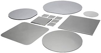
GaAs Wafer
Glass Substrate
Spec
Other Substrate
Orientation
Finishing
(100)・(110)・(111)~(611)For other orientation and off-orientation,please ask us.
Single side mirror polished, Double sides mirror polished, Epi-ready For othertreatment,please ask us.
Thickness
2inch: 350or500um, 3inch: 625um For other thickness,please ask us.
Gallium Nitride, GaN
wide bandgap III-V semiconductor with direct bandgap 3.5 eV wide; among very few semiconductors capable of generating blue radiation, GaN is used for blue LEDs and lasers; intrinsically n-type semiconductor but can be doped p-type; GaN is formed as an epitaxial layer; Lattice mismatch remains a problem, creating a high defect density. Incorporation of Indium (InxGa1-xN) allows control of emission from green to violet (high and low In content respectively). GaN can also be used in UV detectors that do not respond to visible light. GaN has a Wurtzite(W) or Zinc Blend(ZB) crystal structure. Lattice constant [A] 3.189(W) 5.186(ZB); Density[g/cm3] 6.15(W) 6.15(ZB); Atomic concentration [cm-3] 8.9 x 10²²(W) 8.9 x 10²²(ZB); Melting point [oC] 2,500(W) 2,500(ZB); Thermal conduct.[W/cm oC] 1.3(W) 1.3(W); Thermal expansion coefficient[oC-1] ~1x10⁻⁶; Dielectric constant (static) 8.9(W) 9.7(ZB); Refractive index 2.4(W) 2.3(ZB);
GaP
Crystal structure zinc blend; Lattice constant [A] 5.45; Density [g/cm3] 4.14; Atomic concentration [cm-3] 4.94 x 10²²; Melting point [oC] 1457; Thermal conductivity [W/cm oC] 1.1; Thermal expansion coefficient[1/oC] 4.65x10⁻⁶; Dielectric constant 11.1; Refractive index 3.02; Energy gap [eV] 2.26; Type of energy gap: direct; Electron mobility [cm2/V sec] 250; Hole mobility [cm2/V sec] 150;
Spec
MOCVD-deposited GaN
Type/Dopant
Diameter
Orientation
Finishing
Thickness
N-type/S,Si,P-type/Zn Un-doped also available
2inch ~ 3inch
(100), (111), (110) Other special orientation or off angle also available.
Single side mirror polished, Double sides mirror polished, as-cut
250-1000um
Indium Phosphide, InP
Compared with GaAs or GaP,InP single crystal substrate has larger lattice constant,therefore it is possible to grow epitaxial like InGaAs,AlInAs,InGaAsP and AlGAINAs etc by matching the lattice on substrate(unifying lattice constant).
By combining these materials,it's possible to produce light-receiving and emitting device for light communication, super-fast transistor and resonance tunneling diode.
Spec
Type/Dopant
N-type/S・Sn・Un-doped, P-type/Zn, Semi-Insulating/Fe
Diameter
2inch
Orientation
(100)・(110)・(111)~(611) For other orientation and off-orientation,please ask us.
Finishing
Single side mirror polished, Double sides mirror polished, Epi-ready For other treatment,please ask us.
Thickness
2inch: 350or500um,For other thickness,please ask us.
Others
For career concentration, resistivity, mobility, it can be specified within the allowable range.
Gallium Antimondide, GaSb
Gallium Antimondide (GaSb) is a single crystal grown by special LEC method,used in infrared detector,LED,laser,transistor and thermostat photovoltaic system etc.
As typified by GaSb, III-V group compound semicoductors are direct transition semiconductor,the bandgap of which is smaller than Si semiconductor, it can also tranfer the electromagnetic wave (length of 0.8um ~2.2um) in near-infrared area to electricity.
Technically,solar cell based on GaSb is very difficult however research on II-VI group epi by MBE to GaSb substrate is now under study.
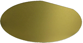
GaSb Wafer
Indium Aesenide, InAs
InAs (Indium Aesenide) of III-V group compound is a single crystal made by LEC method.
Wafer substrate is thinly sliced from single crystal ingot,then polished to epi-ready. InAs can be used
in different wide areas such like measurement and analysis as infrared detector element by performing
epitaxial layer to wafer substrate.
Spec
Type/Dopant
N-type/S, Un-doped, P-type/Zn
Diameter
2inch ~ 3inch
Orientation
(100)・(110)・(111)~(611) For other orientation and off-orientation,please ask us.
Finishing
Single side mirror polished, Double sides mirror polished, Epi-ready For other treatment,please ask us.
Thickness
2inch: 500um, 3inch: 625um For other thickness,please ask us.
Others
For career concentration, resistivity, mobility, it can be specified within the allowable range.
Indium Antimonide, InSb
InSb is a direct transition semiconductor with a narrow bandgap of 0.17eV (room temperature),mainly used as infrared detector element for infrared thermographic,thermal imaging camera and homing missile;hall element and magnetoresistance effect element etc.
Spec
Type/Dopant
N-type/Te, Un-doped, P-type/Ge
Diameter
2inch ~ 4inch
Orientation
(100)・(110)・(111)~(611) For other orientation and off-orientation,please ask us.
Finishing
Single side mirror polished, Double sides mirror polished, Epi-ready For other treatment,please ask us.
Thickness
2inch :625um, 3inch :800/900um, 4inch 1000um For other thickness,please ask us.
Others
For career concentration, resistivity, mobility, it can be specified within the
allowable range.
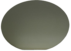
Indium antimonide
II-VI Semiconductors
II-VI group semiconductor is made by II group elements and VI group elements. Magnesium, Zinc, Cadmium and Hydrargyrum from II group and,Oxygen,Sulfur,Tellurium and Selenium from VI group are popularly used elements.
Compounds combined by these elements such as ZnO,CdTe,ZnSe and ZnS.
II-VI group semiconductor has many features like strong ion crystalline,hard but many of them are fragile,however bandgap can be greatly changed by changing the composion.
The material which has a bandgap correspond to visible light and infrared area can be used as material for light emmiting and receiving.
Product
CdSe
CdS
ZnSe
ZnTe
ZnS
Zinc selenide
The Summit-Tech Company is an ISO:9001-2015 certified company. Copyright ©1996-2016 Summit-Tech Company® All rights reserved.