Si Wafer
SOI Wafer
SOI Technology


Macroporous
Other Substrate
SOI is the abbreviation for Silicon-on-insulator, a structure where a thin silicon layer lies atop an insulator, such as silicon dioxide, that may be a silicon or other substrate. This allows for isolation of the active silicon layer containing circuit structures from the bulk substrate (or handle wafer), permitting improved device performance for CMOS devices and more flexible integration schemes for electronic, MEMS and MOEMS devices.
SOI SPECS
Nominal Product Capabilities
ITEM
SIMOX
BESOI
Simbond
Smart-Cut
Wafer Size
4",5",6",8"
4",5",6",8"
6",8"
8"
TOP Si Layer
Thickness w/epi≦15μm
Uniformity
≦230 nm
1-150 μm
±2.5%
±0.5 μm
≦1-190 nm
≦1.5 μm
±5%
±5%
BOX Layer
Thickness
Uniformity
≦400 nm
≦3.5 μm
≦3 μm
≦3 μm
±2.5%
±2.5%
±2.5%
±2.5%
LPD (≧1.6μm)
≦200
≦200
≦200
≦200
Surface Metals (atom.10-2)
≦5E10
≦5E10
≦5E10
≦5E10
SIMOX
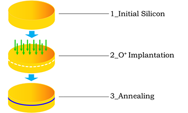
SIMOX, which stands for Separation by Implantation of Oxygen, is a process that Simgui uses to create an insulating layer between the layers of a bulk silicon wafer. There are two essential stages of the process: ion implantation and annealing.
In the implantation stage, oxygen ions are implanted in the silicon wafer and react with the silicon to form silicon dioxide precipitates. However, the implantation causes considerable damage to the wafer and the layer of silicon dioxide precipitates is not continuous. Thus high-temperature annealing helps repair the damage and form the oxide precipitates into a continuous layer. Now the silicon's quality is restored and the buried oxide (BOX) layer can act as a highly effective insulator.
Bonding
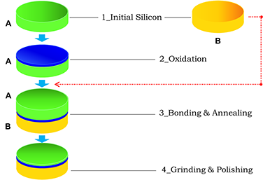
By using bonding chemistry between silicon (Si) and silicon dioxide(SiO2) or between SiO2 and SiO2 effectively, two Si wafers are tightly bonded with a SiO2 layer as an insulator inside the bonded pair. After one side of the Si bulk is thinned down properly with a desired active Si layer thickness, bonded SOI wafers are obtained.
The fabrication process is accomplished by three basic steps. The first step is to mate a thermally oxidized wafer on a non-oxidized wafer at room temperature. The second step is to anneal the bonded pair to increase bonding strength. The third step is to thin down one side of the bonded pair to an appropriate thickness by grinding, etching and polishing.
Simbond
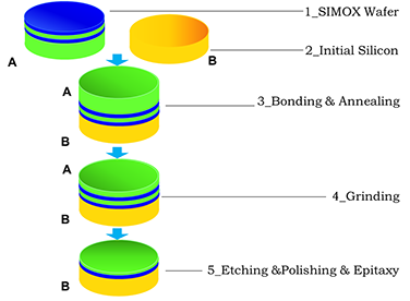
Derived from conventional wafer bonding and ion-implantation technologies comes another method called Simbond that Simgui originates in preparation of SOI materials.
The ion-implantation provides a well distributed ion-implanted layer. This layer serves as a chemical etch stop layer, which allows for an excellent uniformity control on the thickness of the device layer before a final polish process. The innovated process can produce high quality SOI wafer with superior SOI uniformity and thick BOX layer.
Smart-cut ™ Technology
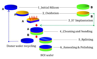
Smart Cut ™ technology is the world leader in fabrication of SOI materials. The fabrication process is accomplished by five basic steps.
1. Thermal oxidation.
2. Hydrogen Implantation.
3. Cleaning&Boning.
4. Splitting.
5. Annealing& CMP touch polishing.
The Summit-Tech Company is an ISO:9001-2015 certified company. Copyright ©1996-2016 Summit-Tech Company® All rights reserved.