
Si Wafer
SOI Wafer
Sapphire Wafer
III-V Wafer
GeSn thin film Wafer
Glass Substrate
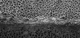
Macroporous
Other Substrate
Porous silicon was accidentally discovered by Uhlir at Bell Laboratories in the mid 1950s. He was trying to develop a means to electrochemically machine silicon wafers for use in microelectronic circuits. He found that under the appropriate conditions of applied current and solution composition, the silicon did not dissolve uniformly but instead fine holes were produced, which propagated primarily in the <100> direction in the wafer. Since this did not provide the smooth polish desired, these curious results were reported in a Bell labs technical note and the material was pretty much ignored. In the 1970s and 1980s a moderate level of interest arose because the high surface area of porous Si was found to be useful as a model of the crystalline Si surface in spectroscopic studies, as a precursor to generate thick oxide layers on Si, and as a dielectric layer in capacitance-based chemical sensors. Then, in the late 1980s, Leigh Canham at the Defense Research Agency in England reasoned that the diaphanous Si filaments generated when the pores become large and numerous enough to overlap might display quantum confinement effects. This intuition turned out to be correct, and the electrochemically etched material was reported to fluoresce with a bright red-orange color. As expected from the quantum confinement relationship, this color is at an energy that is significantly larger than the bandgap energy for bulk Si, which occurs in the infrared region of the spectrum.
With the discovery of efficient visible light emission from porous Si came an explosion of work focused on creating Si-based optoelectronic switches, displays, and lasers. Problems with the material’s chemical and mechanical stability and its disappointingly low electroluminescence efficiency led to a waning of interest by the mid 1990s. In the same time period, the unique features of the material- its large surface area within a small volume, its controllable pore sizes, its convenient surface chemistry, and its compatibility with conventional silicon microfabrication technologies-inspired research into applications far outside of optoelectronics. Of particular relevance to our research are the biomedical and sensor properties of the material.
Applications of porous silicon
Application area
Optoelectronics
Micro-optics
Energy conversion
Environmental monitoring
Role of porous silicon
LED
Waveguide
Field emitter
Optical memory
Fabry-Pérot Filters
Photonic bandgap structures
All optical switching
Antireflection coatings Photo-electrochemical cells
Gas sensing
Efficient electroluminescence
Key property
Tunability of refractive index
Hot carrier emission
Non-linear properties
Refractive index modulation Regular macropore array Highly non-linear properties
Low refractive index
Photocorrosion cells
Ambient sensitive properties
Microelectronics
Micro-capacitor
Insulator layer
Low-k material
High specific surface area
High resistance
Electrical properties
Wafer technology
Buffer layer in heteroepitaxy
Variable lattice parameter
SOI wafers
High etching selectivity
Micromachining
Thick sacrificial layer
Highly controllable etching
Biotechnology
Tissue bonding
Biosensor
Tunable cht emical reactivity Enzyme immobilization
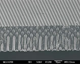
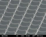
MakroPor

Interpore distance
1,5 µm
4,2 µm
12 µm
Pore diameter
0,8 - 1 µm
2 - 2.5 µm
5 - 6µm
Pore length
200 µm
500 µm
500 µm
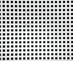
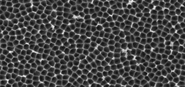
SmartPor

FlexiPor

Interpore distance
65 nm
125 nm
480 nm
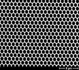
Interpore distance
20 ± 8 nmt
100 ±15 nm
200 ±25 nm
Pore diameter
25 nm
40 nm
180 nm
Pore diameter
160 ± 10 nm
200 ± 15 nm
220 ± 25 nm
Pore length
50 µm or 100 µm
50 µm or 100 µm
50 µm or 100 µm
Pore length
50 µm or 100 µm
50 µm or 100 µm
50 µm or 100 µm
The Summit-Tech Company is an ISO:9001-2015 certified company. Copyright ©1996-2016 Summit-Tech Company® All rights reserved.