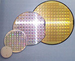
A wafer, also called a slice or substrate, is a thin slice of semiconductor material, such as a crystalline silicon, used in electronics for the fabrication of integrated circuits and in photovoltaics for conventional, wafer-based solar cells. The wafer serves as the substrate for microelectronic devices built in and over the wafer and undergoes many microfabrication process steps such as doping or ion implantation, etching, deposition of various materials, and photolithographic patterning. Finally the individual microcircuits are separated (dicing) and packaged.

Standard wafer sizes
Silicon wafers are available in a variety of diameters from 25.4 mm (1 inch) to 300 mm (11.8 inches). Semiconductor fabrication plants (also known as fabs) are defined by the diameter of wafers that they are tooled to produce. The diameter has gradually increased to improve throughput and reduce cost with the current state-of-the-art fab using 300 mm, with a proposal to adopt 450 mm.Intel, TSMC and Samsung are separately conducting research to the advent of 450 mm "prototype" (research) fabs, though serious hurdles remain.
2-inch (51 mm), 4-inch (100 mm), 6-inch (150 mm), and 8-inch (200 mm) wafers
1-inch (25 mm)
2-inch (51 mm). Thickness 275 µm.
3-inch (76 mm). Thickness 375 µm.
4-inch (100 mm). Thickness 525 µm.
5-inch (130 mm) or 125 mm (4.9 inch). Thickness 625 µm.
150 mm (5.9 inch, usually referred to as "6 inch"). Thickness 675 µm.
200 mm (7.9 inch). Thickness 725 µm.
300 mm (11.8 inch). Thickness 775 µm.
450 mm (17.7 inch). Thickness 925 µm (proposed).
2-inch (51 mm), 4-inch (100 mm), 6-inch (150 mm), and 8-inch (200 mm) wafers
The Summit-Tech Company is an ISO:9001-2015 certified company. Copyright ©1996-2016 Summit-Tech Company® All rights reserved.
